Address
Building A1, Runteng Industrial Park, No. 4 Xishan Road, Longteng Community, Shiyan Subdistrict, Bao'an District, Shenzhen 518000, China
Work Hours
Monday to Saturday: 09:00 – 23:00 (UTC+8)
Sunday: closed
Address
Building A1, Runteng Industrial Park, No. 4 Xishan Road, Longteng Community, Shiyan Subdistrict, Bao'an District, Shenzhen 518000, China
Work Hours
Monday to Saturday: 09:00 – 23:00 (UTC+8)
Sunday: closed

Request a quote
AUTOMATIC SOLDER PASTE PRINTER
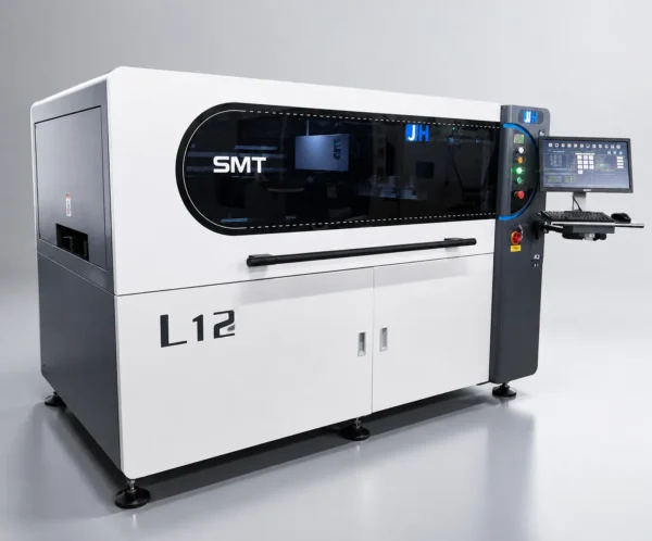
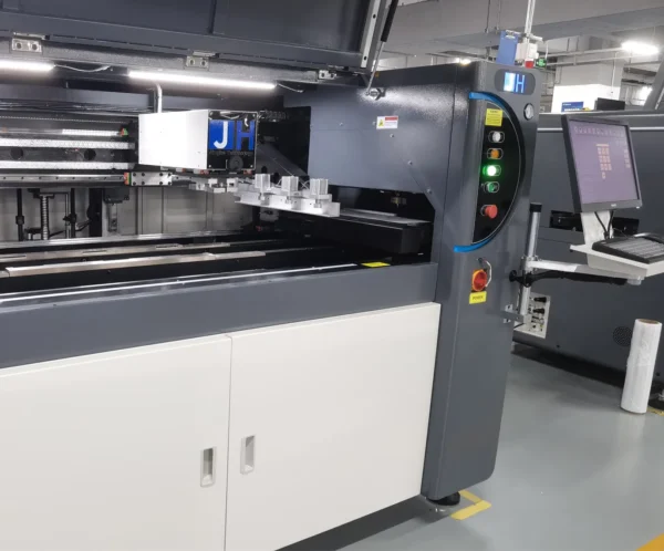
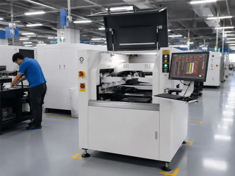
The JHIMS L12 solder paste printer prints PCB boards up to 1200×350mm with ±0.025mm accuracy on stencil frames up to 1500×750mm. Engineered for miniLED, semiconductor and new energy manufacturing — with 01005 ultra-fine printing, three-stage snap-mode demolding and built-in 2D solder paste inspection.
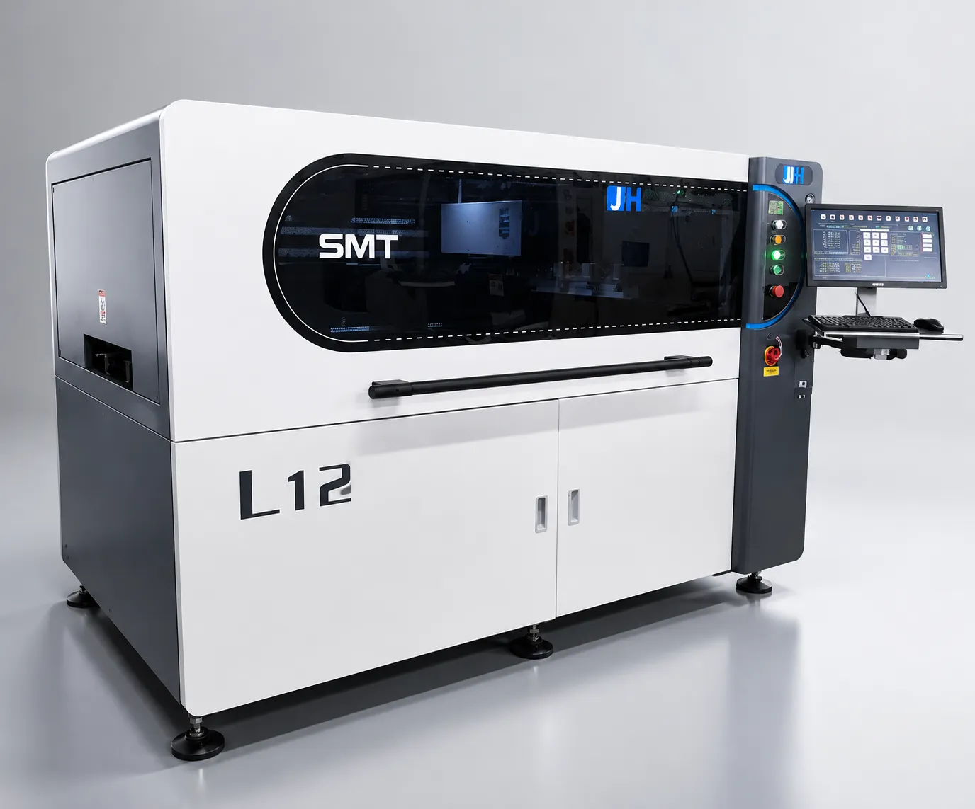
The JHIMS L12 solder paste printer is a fully automatic visual printer built for extra-large miniLED modules, semiconductor packaging, and new energy PCB manufacturing. This automatic visual solder paste printer supports PCB sizes from 50×50mm up to 1200×350mm and stencil frames up to 1500×750mm, with a maximum board weight of 7kg. Featuring a 1.3-megapixel CCD vision system with up/down imaging and stepless light adjustment, ±0.025mm printing accuracy, ±0.015mm repeat positioning accuracy, and three-stage snap-mode demolding, the L12 delivers precise, repeatable paste deposition for 01005 components and 0.25mm-pitch ultra-fine circuits.
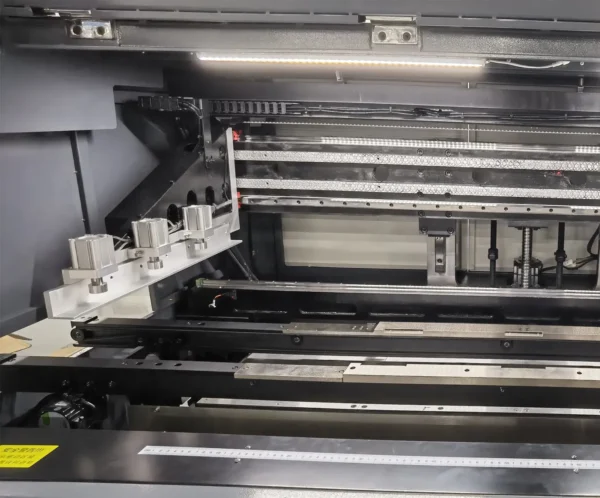
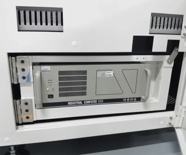
The L12 automatic visual solder paste printer is built for 24/7 industrial production with a heavy-duty frame rated for 1500kg machines, a one-section high-speed transport track (max 1500mm/s), and an industrial PC control system supporting Industry 4.0 MES connectivity.
Applications: The L12 solder paste printer is ideal for miniLED modules, semiconductor packaging boards, new energy battery management systems (BMS), and large-format PCB assemblies up to 1200×350mm.
Handles PCB sizes from 50×50mm up to 1200×350mm and stencil frames up to 1500×750mm with a maximum board weight of 7kg — built for miniLED modules, semiconductor packaging, and new energy boards.
1.3-megapixel CCD camera with up/down imaging and stepless light adjustment. 10×8mm field of view and 150ms capture cycle deliver fast, reliable fiducial alignment for 01005 components and 0.25mm-pitch circuits.
Repeat positioning accuracy of ±0.015mm combined with precise squeegee pressure control (0.5–25kg) ensures consistent, uniform solder paste deposition across the full print area.
Programmable release distance (0–20mm) and speed (0–20mm/sec) with three-stage snap-mode separation guarantee clean paste release from even the smallest stencil apertures, reducing defects on ultra-fine features.
Detects low tin, missing print, and solder bridging in real time before reflow. Automatic compensation for offset and automatic stencil cleaning keep quality consistent run after run.
Dry wipe, wet wipe, and vacuum cleaning modes with automatic stroke generation based on PCB dimensions. Cleaning fluid and paper consumption are auto-generated and manually adjustable.
Standard MES connectivity records SOPs and open equipment data for upload, with customizable Industry 4.0 output. Optional SPI connection, automatic tinning, temperature/humidity detection, and traceability camera.
Brand-new interface with shortcut key operation. Freely configurable permission levels for operators, technicians, and engineers. Safety interlock stops the machine when the door opens.
| Parameter | Specification | Parameter | Specification |
|---|---|---|---|
| Model | L12 | Stencil Frame (Min) | 520×300mm |
| Stencil Frame (Max) | 1500×750mm | Stencil Thickness | 20–40mm |
| Stencil Positioning | Manual positioning | PCB Min Size | 50×50mm |
| PCB Max Size | 1200×350mm | PCB Thickness | 0.4–6mm |
| PCB Warpage | <1% | Board Edge Clearance | 2.5mm |
| Board Height | 25mm | Transport Height | 900±40mm |
| Transport Direction | L→R; R→L; L→L; R→R | Transport Speed | Max 1500mm/s (Programmable) |
| Transport Mode | One-section transport track | PCB Support System | Magnetic Pin / Adjustable Lift Table / Support Block |
| Max PCB Weight | 7kg | Printing Speed | 10–200mm/sec |
| Printing Pressure | 0.5–25kg | Printing Mode | Single or Double Squeegee |
| Release Distance | 0–20mm | Release Speed | 0–20mm/sec |
| Release Mode | Three-stage snap-mode demolding | Squeegee Type | Steel (Standard), Rubber |
| Repeat Position Accuracy | ±0.015mm | Printing Accuracy | ±0.025mm |
| Cycle Time | <15s (Excl. Print & Clean) | Changeover Time | <5 Minutes |
| Cleaning Method | Dry / Wet / Vacuum (spray) | Cleaning Position | Right-side cleaning |
| Cleaning Speed | 10–200mm/sec | CCD Field of View | 10×8mm |
| Camera Type | 1.3MP digital camera | Camera System | Up/down imaging, stepless light adjustment |
| Camera Cycle Time | 150ms | Fiducial Mark Types | Square, Circle, Triangle, Diamond, Cross, Pad, Hole |
| Mark Size | 0.1–6mm | Mark Number | Max 4 |
| 2D Detection | Low tin / Missing print / Solder bridge | Traceability System | Camera scan code, 2.5×2.5–8×8mm |
| Air Required | 4–6Kgf/cm² | Air Consumption | ~5L/min |
| Working Temperature | -20℃~45℃ | Working Humidity | 30%~60% |
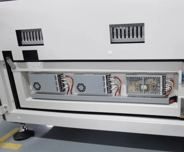
| Power Input | AC 220±10%, 50/60Hz, 1Φ, 3.5KW | Control Method | PC Control |
| Machine Dimensions | 2200(L)×1200(W)×1500(H)mm | Machine Weight | ~1500Kg |
The JHIMS L12 Extra-large fully automatic visual solder paste printer is a versatile workhorse deployed across mission-critical electronics manufacturing sectors worldwide.
The L12 is purpose-built for miniLED module printing, where thousands of tiny solder pads must be filled with consistent paste volume across large panel sizes. Its 1200×350mm PCB capacity and 1500×750mm stencil frame support full LED panel arrays, while ±0.025mm accuracy and 0.25mm-pitch capability handle the ultra-fine pad geometries of miniLED COB and COG processes. The 2D inspection system catches low-tin and bridging defects on individual micro-pads before reflow, protecting yield on high-value LED panels.
Semiconductor substrate and packaging boards demand precise, repeatable paste deposition on fine-pitch pads with minimal contamination risk. The L12 delivers 01005 component capability with ±0.015mm repeat positioning, three-stage snap-mode demolding for clean release from fine apertures, and a traceability camera (2.5×2.5–8×8mm code range) for full lot-level process tracking. The standard MES interface supports the data documentation required for semiconductor quality systems.
New energy battery management systems (BMS), inverters, and power electronics use large boards with thick copper and heavy components. The L12 handles boards up to 1200×350mm weighing up to 7kg with a magnetic pin / adjustable lift table support system for stable, flat printing. Programmable squeegee pressure up to 25kg ensures complete aperture fill on high-current traces, and the one-section transport track moves heavy boards smoothly at up to 1500mm/s.
For EMS providers running mixed production, the L12’s under-5-minute changeover and automatic program recall keep lines productive across frequent product switches. The smart UI with role-based access separates operator, technician, and engineer permissions, while the standard MES system records SOPs and equipment data for Industry 4.0 reporting — ideal for automotive Tier-1 traceability requirements.
Understanding solder paste printing technology is essential for optimizing your SMT assembly process. Below is a comprehensive technical reference for engineers and process managers.
Solder paste is a shear-thinning non-Newtonian fluid. The L12’s programmable printing speed (10–200mm/sec) and pressure (0.5–25kg) let you match squeegee dynamics to paste viscosity — typically 800–1200 kcps at the print head. Start pressure at roughly 0.5kg per 100mm of squeegee length and adjust in 0.5kg steps. For fine-pitch work (0.25mm pitch and below), reduce print speed and increase pressure slightly to ensure complete aperture fill without paste skipping.
L12 supports stencil frames from 520×300mm to 1500×750mm with 20–40mm frame thickness. For large panels, aperture design determines release efficiency: maintain area ratios ≥0.66 and aspect ratios ≥1.5. Use laser-cut stainless steel stencils with electropolished aperture walls and nano-coating for fine-pitch miniLED and semiconductor work. Tension the mesh evenly across the large frame to prevent sagging in the center, which causes paste thickness variation.
Demolding is the critical moment when the stencil separates from the printed board. The L12’s three-stage snap-mode system separates release into controlled phases with adjustable distance (0–20mm) and speed (0–20mm/sec). For fine-pitch apertures, use a slower, multi-stage release to let paste pull cleanly from aperture walls; for standard SMT work, a faster snap improves throughput. The staggered separation prevents the “vacuum effect” that causes paste lifting on large-area prints.
The L12’s built-in 2D inspection detects low tin, missing print, and solder bridging in real time. Acceptable thresholds: paste area variation within ±15%, X/Y offset within ±50μm for standard components and ±25μm for fine-pitch. The system triggers automatic offset compensation and can trigger stencil cleaning when low-tin is detected. Track inspection results by lot using the traceability camera to build an SPC database for continuous process improvement.
Maximize your L12 performance with these manufacturing operation and maintenance guidelines.
1. Verify air supply at 4–6Kgf/cm² through the 8mm line. 2. Check squeegee blades for wear (steel standard, rubber optional). 3. Run a dry cleaning cycle to remove residual paste. 4. Confirm conveyor width and support pins for the first board. 5. Verify fiducial marks are clean for vision alignment. 6. Check solvent and cleaning paper levels. 7. Print a test board and inspect with the 2D system before production.
Weekly: Clean guide rails and ball screws, check belt tension, inspect air filters, verify squeegee parallelism. Monthly: Lubricate linear guides, calibrate squeegee pressure, verify CCD alignment and lighting consistency. Quarterly: Full system calibration, replace cleaning paper and vacuum filters, update PC software, inspect the transport track for wear. Annually: Comprehensive service by a JHIMS-certified engineer, including full accuracy verification.
1. Use magnetic pins and the adjustable lift table to support heavy boards (up to 7kg) evenly — never print unsupported panels. 2. Set transport speed below maximum for boards over 800mm long to prevent momentum-related misalignment. 3. Verify board edge clearance (2.5mm) and board height (25mm) for each new product. 4. For warped boards (<1% tolerance), use vacuum suction clamping for flat, stable positioning. 5. Confirm the stencil is tensioned evenly before long runs.
Maintain working temperature between -20℃ and 45℃ with 30–60% humidity. Solder paste pot life is typically 8–12 hours at room temperature — keep unused paste refrigerated and track usage by batch. The L12 requires a dedicated grounding wire and ESD grounding for electrostatic protection, plus a stable AC 220V±10% 50/60Hz 3.5KW supply with a British SS145 (13A) plug. Optional temperature/humidity detection displays ambient conditions in real time.
See exactly where the JHIMS L12 solder paste printer fits in your PCB assembly process and how it integrates with upstream and downstream equipment.
The L12 is the first and most critical step in the SMT assembly line — print quality directly determines downstream yield. JHIMS offers complete line integration support for seamless communication with your MES/ERP system.
| Metric | Manual Printing | JHIMS L12 | Advantage |
|---|---|---|---|
| Printing Accuracy | ±0.1mm (operator dependent) | ±0.025mm | 4× Better |
| Repeat Position Accuracy | Not guaranteed | ±0.015mm | Consistent & Repeatable |
| Cycle Time | 25-35 seconds per board | <15 seconds | 2-3× Faster |
| Changeover Time | 15-30 minutes | <5 minutes | 3-6× Faster |
| Quality Inspection | Visual check (subjective) | 2D automatic — 100% inspection | Full Coverage |
| Operators Required | 2-3 operators per shift | 1 operator manages 3-4 printers | 67% Labor Savings |
| Large-Format Boards | 1200×350mm impractical manually | 1200×350mm, up to 7kg | Extra-Large Capability |
| Process Traceability | Paper logs — manual entry | Digital log — Industry 4.0 MES | Fully Traceable |
Based on typical industry benchmarks. Actual results may vary by application and operating conditions.
Based on the quotation we prepare for your L12 solder paste printer. Enter your current production parameters to calculate how quickly the L12 pays for itself.
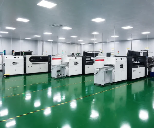
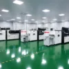
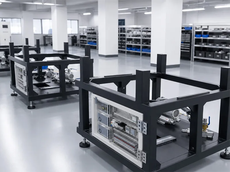
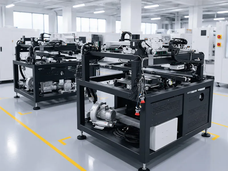
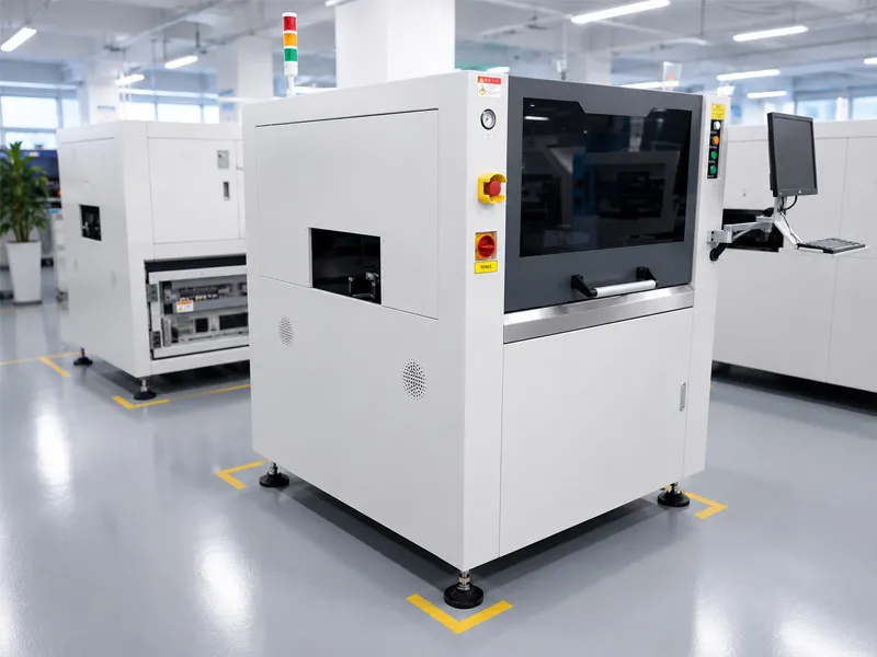
Tour our state-of-the-art manufacturing facility in Shenzhen, China. Every JHIMS L12 solder paste printer is assembled, calibrated, and tested under rigorous quality control standards before shipment.
Watch the JHIMS L12 solder paste printer performing real-world production tasks. All videos are hosted on YouTube for fast, reliable streaming worldwide.

CUSTOMER SUCCESS STORIES
Real deployments of the JHIMS L12 solder paste printer across four continents — from turnkey SMT lines to high-speed LED display production. Every project shipped, installed and supported by the JHIMS team.
 SMT LINE
Full DDP turnkey delivery — YSM10, L5 solder paste printer and F8 reflow oven, engineered, installed and commissioned as one automated line.
 SOLDER PASTE PRINTING
JHIMS L5 automatic printer deployed for an Indian OEM — ±0.01mm precision, full automation and measurable cost reduction in daily production.
 LED DISPLAY
Shenzhen LED display maker scaled output with YSM40R placement — 145K CPH throughput and a shorter, leaner production line.
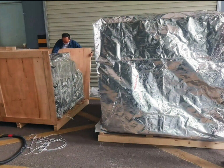 LED MANUFACTURING
Spanish LED manufacturer runs YSM20R placement 24/7 — two years of continuous operation with zero breakdowns and +30% efficiency.
LEARNING CENTER
Practical guides, case studies and reference material about the L12 solder paste printer, solder paste printing and process optimization, written by JHIMS engineers — from procurement strategy to production troubleshooting.
Reference videos: How to Use 1.2m Fully Automatic PCB Printer – Step-by-Step; JHIMS | SMT PCB Solder Paste Printer & Screen Stencil Printing Machine #PCB Printer; PCBA solder automatic printer |Automatic solder printer made in China #smt printer #solder printer.
| Weight | 1500 kg |
|---|---|
| Dimensions | 2200 × 1200 × 1500 mm |