Address
Building A1, Runteng Industrial Park, No. 4 Xishan Road, Longteng Community, Shiyan Subdistrict, Bao'an District, Shenzhen 518000, China
Work Hours
Monday to Saturday: 09:00 – 23:00 (UTC+8)
Sunday: closed
Address
Building A1, Runteng Industrial Park, No. 4 Xishan Road, Longteng Community, Shiyan Subdistrict, Bao'an District, Shenzhen 518000, China
Work Hours
Monday to Saturday: 09:00 – 23:00 (UTC+8)
Sunday: closed

Request a quote
AI-POWERED SMT AOI
Achieve 99.5% inspection accuracy with deep learning AI that reduces false positives by 95%. A 5MP industrial camera at 12µm resolution delivers 3-5 FOV/sec throughput, detecting 50+ defect types from 0201 chips to large BGAs — trusted by 2,456+ manufacturers in 30+ countries across automotive, consumer electronics and medical device industries.
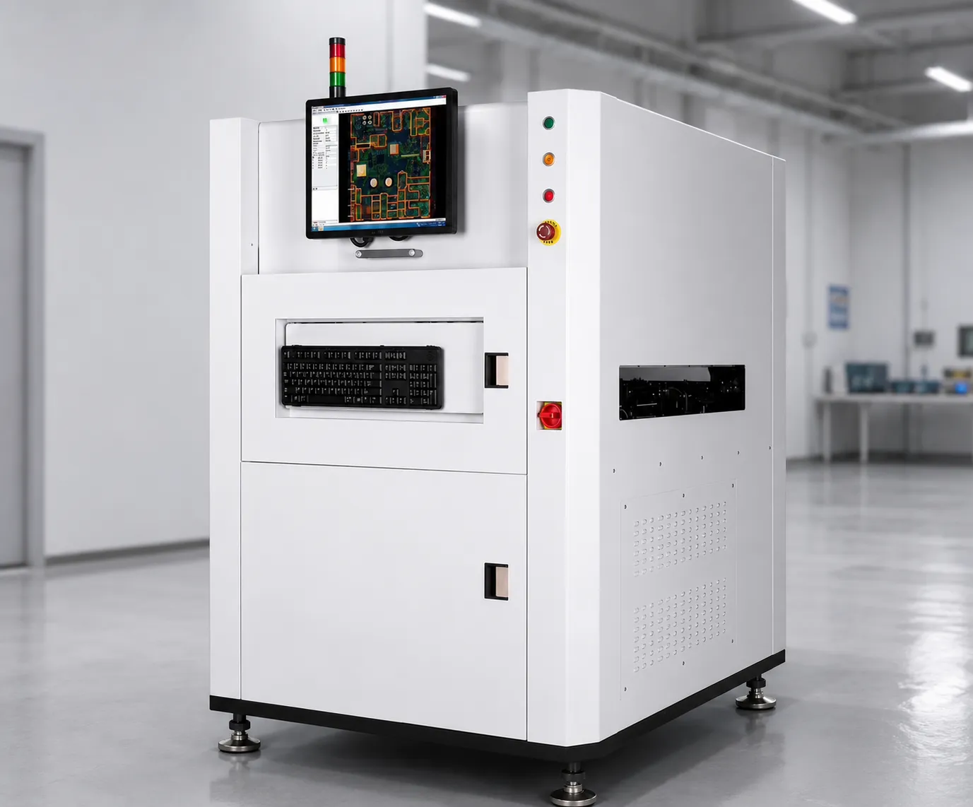
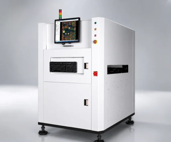
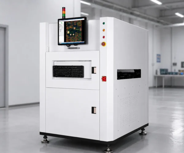
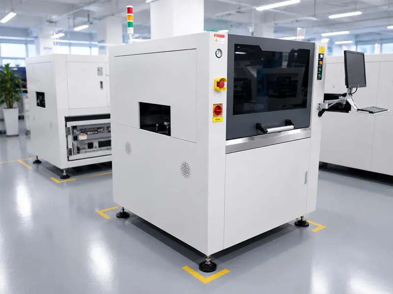
JHIMS XI-2000 AI-Powered SMT AOI Machine
The JHIMS XI-2000 is a next-generation inline SMT AOI machine that combines a 5MP industrial-grade Basler camera with deep learning AI to achieve 99.5% inspection accuracy. As an automatic optical inspection machine designed for high-mix, high-volume PCB assembly, the XI-2000 detects over 50 defect types across 0201 chips, fine-pitch BGAs, QFPs, connectors and through-hole components. At 3-5 FOV per second, this AOI inspection machine keeps high-volume SMT lines moving without sacrificing accuracy. Unlike conventional 2D AOI systems that rely on static rule-based algorithms, the XI-2000’s contextual AI engine learns from your production data to distinguish real defects from acceptable process variations. This reduces false positives by 95%, freeing engineers to focus on genuine process improvements.
Engineered with premium components from Basler (Germany), Panasonic/Mitsubishi (Japan), THK/HIWIN (Japan/Taiwan), and Keyence/Omron (Japan), the XI-2000 delivers industrial-grade reliability for 24/7 production environments.
Applications: Automatic optical inspection for automotive electronics, medical devices, consumer electronics, industrial automation, telecommunications, LED manufacturing, new energy/BMS, aerospace and defense, semiconductor packaging and home appliance PCB assembly.
Contextual AI engine trained on millions of PCB images reduces false positives by 95% compared to rule-based 2D AOI systems. It continuously learns from production data to adapt to process variation, board warpage and component tolerance changes without manual reprogramming.
Industrial-grade 5-megapixel Basler camera with telecentric optics delivers 12µm per pixel resolution across a 36.7×30.7mm field of view. Reliably inspects 0201 chip components, 0.3mm pitch BGAs and ultra-fine-pitch QFP leads that lower-resolution systems miss.
Adds volumetric solder measurement for detecting insufficient solder, excess solder, lifted leads and component coplanarity issues — covering the 3D defects that pure 2D AOI systems cannot see.
Multi-angle illumination eliminates shadows on tall components and improves contrast for reflective leads, dark PCBs and low-profile parts. Each channel is software-tunable for per-board lighting recipes.
Detects missing parts, offset, polarity errors, bridges, insufficient solder, tombstones, lifted leads, foreign material, wrong components, solder balls, component cracks and PCB substrate defects — from 0201 chips to large BGAs.
Standard REST API and database connector push inspection data into MES/ERP for full traceability. Real-time SPC dashboards and defect pareto reports keep your quality team informed.
High-throughput inspection at 3-5 fields of view per second never bottlenecks your SMT line — up to 600 boards/hour depending on board complexity.
AI-assisted programming with automatic component library matching cuts new product introduction from 4-8 hours to under 30 minutes for most boards.
| Parameter | Specification | Parameter | Specification |
|---|---|---|---|
| Model | XI-2000 Online SMT AOI | Maximum PCB Size | 650 × 560 mm |
| Camera | 5 MP Industrial Camera (Basler) | Optical Resolution | 12 µm |
| Field of View (FOV) | 36.7 × 30.7 mm | Inspection Speed | 3-5 FOV/sec |
| Lighting System | 4-Channel High-Grayscale LED | PCB Thickness | 0.6 – 6 mm |
| Top Clearance | 45 mm | Bottom Clearance | 50 mm |
| Conveyor Height | 900 ± 20 mm | Conveyor Direction | Left-to-Right (SMEMA standard) |
| Power Supply | AC 220V, 50/60 Hz, 1.8 KVA | Air Supply | 5 bar (0.5 MPa) |
| Operating Temperature | 5-40°C | Operating Humidity | 25-80% RH (non-condensing) |
| Machine Dimensions | 1200 × 1200 × 1840 mm (L×W×H) | Net Weight | 900 kg |
| Communication Interface | Standard SMEMA + RJ45 Ethernet | MES/ERP Integration | REST API, database connector |
| Defect Types Detected | 50+ types (see detection section) | Inspection Accuracy | 99.5% (verified at 0201 capability) |
| False Positive Rate | < 5% (with AI learning) | MTBF | 50,000 hours |
| 3D Profiling (Optional) | Solder height, coplanarity, warpage | Certifications | ISO 9001:2015, CE, RoHS |
Every JHIMS XI-2000 is built with world-class components. We source only from industry-leading brands to ensure long-term reliability and precision.
The JHIMS XI-2000 AI-Powered SMT AOI Machine is a versatile workhorse deployed across mission-critical electronics manufacturing sectors worldwide.
The XI-2000 meets rigorous automotive quality requirements with traceability to individual component level. It detects micro-cracks in MLCC capacitors, insufficient solder on high-current BMS traces and lifted leads on engine-control connectors. AI models are trained on automotive acceptance criteria including IPC-A-610 Class 3 and customer AQL limits.
Medical electronics demand zero-defect manufacturing with complete traceability documentation. The XI-2000 records inspection images and results for every board, supporting FDA 21 CFR Part 11 electronic record compliance and full batch genealogy reporting.
High-mix smartphone and wearable lines benefit from sub-30-minute NPI programming and 3-5 FOV/sec throughput. The AI engine distinguishes acceptable process variation from real defects on dense mainboards, cutting false calls that slow down operator verification.
Mission-critical telecom PCBs with large BGAs, high-pin-count connectors and mixed SMT/THT assembly demand zero-defect quality. The XI-2000 provides complete traceability at production volumes exceeding 50,000 boards monthly.
LED driver boards and backlight strips benefit from 4-channel lighting recipes tuned for reflective aluminum substrates, eliminating false calls from conformal coating reflections.
Battery management system PCBs require strict inspection of high-current traces and solder joints. The XI-2000 detects insufficient solder on thick copper traces and lifted leads on connectors with AI-verified confidence.
Understanding AOI inspection technology is essential for optimizing your SMT assembly process. Below is a comprehensive technical reference for engineers and process managers.
Rule-based systems flag anything outside static thresholds, causing 30-40% false positive rates. The XI-2000 contextual AI understands normal process variation — slightly darker solder joints, minor component color differences, normal placement tolerances — and reduces false positives by 95% while catching defects legacy systems miss.
The XI-2000 detects 50+ defect types with AI-verified confidence: missing components down to 0201 size (99.8% confidence), component offset or misalignment from ±0.05mm (99.5%), polarity errors on 0201 markings (99.7%), solder bridges from 0.05mm width (99.3%), insufficient solder or dry joints (98.9%), tombstoning on 0201 parts (99.9%), bent or lifted pins on 0.3mm-pitch QFPs (99.2%), foreign material from 0.1mm particles (98.5%), wrong component values (99.0%), solder balls from 0.05mm (98.7%), component body damage from 0.1mm cracks (97.5%) and PCB substrate defects from 0.2mm scratches (97.0%).
Four independently controlled LED channels at different azimuth angles eliminate shadows on tall components and maximize contrast for reflective leads, dark PCBs and low-profile parts. Lighting recipes are stored per board program and recalled automatically at changeover.
Adds true volumetric measurement of solder joints: insufficient solder, excess solder, lifted leads and component coplanarity. Combined with 2D inspection, the 3D channel detects defects that flat 2D imaging cannot resolve, such as gradated bridges and micro-cracks.
Maximize your XI-2000 performance with these manufacturing operation and maintenance guidelines.
AI-assisted programming with automatic component library matching cuts new product introduction from 4-8 hours to under 30 minutes for most boards. The system generates inspection programs directly from CAD/Gerber data with minimal manual tuning.
Standard REST API and database connector make integration straightforward. Inspection results, images and SPC data push into MES/ERP in real time, with support for forced-login operator tracking and full traceability reporting.
Calibration targets ship with each machine for verifying optical resolution and lighting uniformity. Recommended verification: weekly resolution check, monthly full calibration with the NIST-traceable target, and quarterly Gage R&R study.
The XI-2000 is positioned post-reflow as the final quality gate before PCB unloading — catching all assembly defects before boards proceed to test, coating or box-build.
The XI-2000 operates at 3-5 FOV/sec so it never becomes the bottleneck. Optional pre-reflow placement provides early defect detection, enabling rework before solder solidifies — valuable for high-value boards.
| Metric | Manual Printing | JHIMS XI-2000 | Advantage |
|---|---|---|---|
| Inspection Accuracy | 85-90% (fatigue-dependent) | 99.5% | 10-15% Higher |
| False Positive Rate | 15-25% | < 5% | 80% Fewer False Calls |
| Inspection Speed (UPH) | 60-120 boards/hour | 300-600 boards/hour | 5x Faster |
| Min Component Size | 0201 (eyesight limit) | 0201 (0.2×0.1mm) | 4x Finer |
| 3D Defect Detection | Not possible visually | Optional 3D profiling | Infinite Advantage |
| Labor Cost/Month | $2,100 (3 inspectors/shift) | $0 — fully automated | 100% Labor Saving |
| Traceability | Manual paper records | Full MES traceability | Complete Digital Record |
| Shift Coverage | Fatigue after 4-6 hours | 24/7 continuous operation | Non-Stop Operation |
| NPI Programming | 1-2 days per product | < 30 minutes | 48x Faster |
Based on typical industry benchmarks. Actual results may vary by application and operating conditions.
Enter your current production parameters to calculate how quickly the JHIMS XI-2000 pays for itself.
Every JHIMS machine is assembled, calibrated and burn-in tested in our Shenzhen facility, then carefully packed for international delivery.
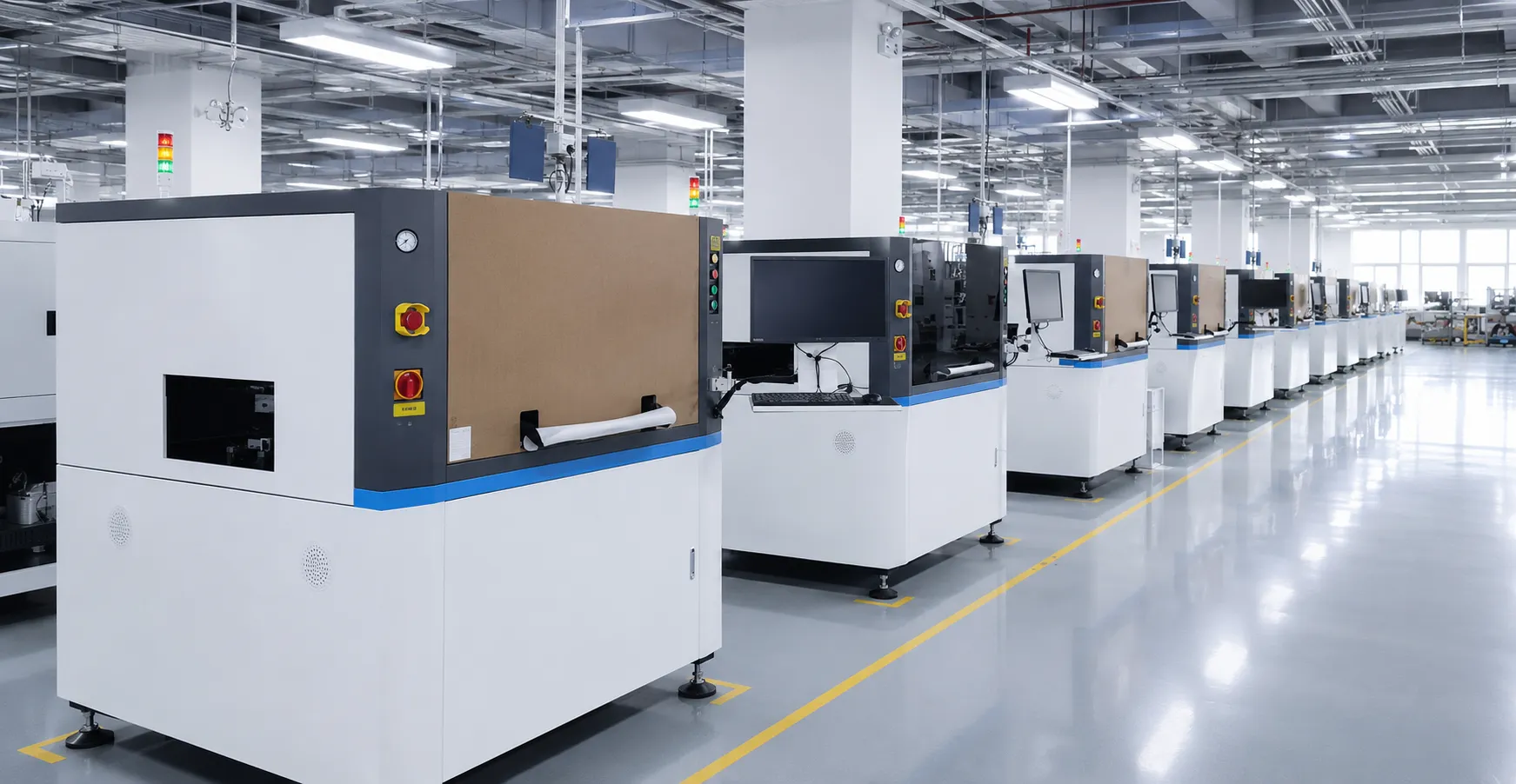
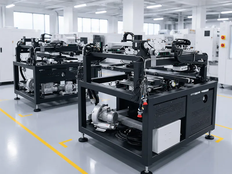
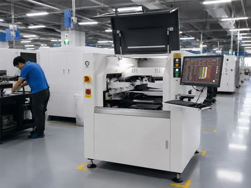
Watch the JHIMS XI-2000 performing real-world production tasks. All videos are hosted on YouTube for fast, reliable streaming worldwide.


CUSTOMER SUCCESS STORIES
Real-world results from SMT and PCB manufacturers who work with JHIMS — an ISO 9001 certified SMT equipment manufacturer — every case links to a verified JHIMS case study.
 LINE AUTOMATION
How a TCL production line cut changeover time by 85% and lifted throughput by 30% with JHIMS automation.
 PCB ASSEMBLY
A Vietnamese EMS provider passed a Toyota supplier audit with zero scratch defects after reconfiguring their PCB line.
 COST REDUCTION
How a Mexican PCB assembly operation reduced labor cost by 67% through SMT line automation.
LEARNING CENTER
Expert guides and real case studies for automatic optical inspection in SMT production, written by JHIMS engineers.
Reference videos: watch the process on YouTube; watch the process on YouTube; watch the process on YouTube.
| Weight | 900 kg |
|---|---|
| Dimensions | 1200 × 1200 × 1840 mm |
| Field of View (FOV) | 36.7 × 30.7 mm |
| Maximum PCB Size | 650 × 560 mm |
| Inspection Speed | 3-5 FOV/sec |
| PCB Thickness | 0.6 – 6 mm |
| Power Supply | AC 220V, 50/60 Hz, 1.8 KVA |
| Lighting System | 4-Channel High-Grayscale LED |