JHIMS XI-2000 SMT AOI Machine | AI-Powered PCB Inspection

Request a quote

XI-2000 — AI-Powered SMT AOI Machine
99.5% Accuracy95% Fewer False Calls5MP @ 12μm3-5 FOV/sec50+ Defect Types
  • 🧠 Deep learning AI classification — adapts to your production data
  • 📷 5MP Basler camera + 4-channel lighting · 0201 to large BGA
  • 🏭 ISO 9001 · CE compliant · 2,456+ clients in 30+ countries · Global after-sales
Request Quote

AI-POWERED SMT AOI

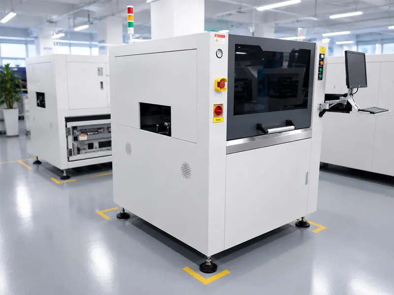
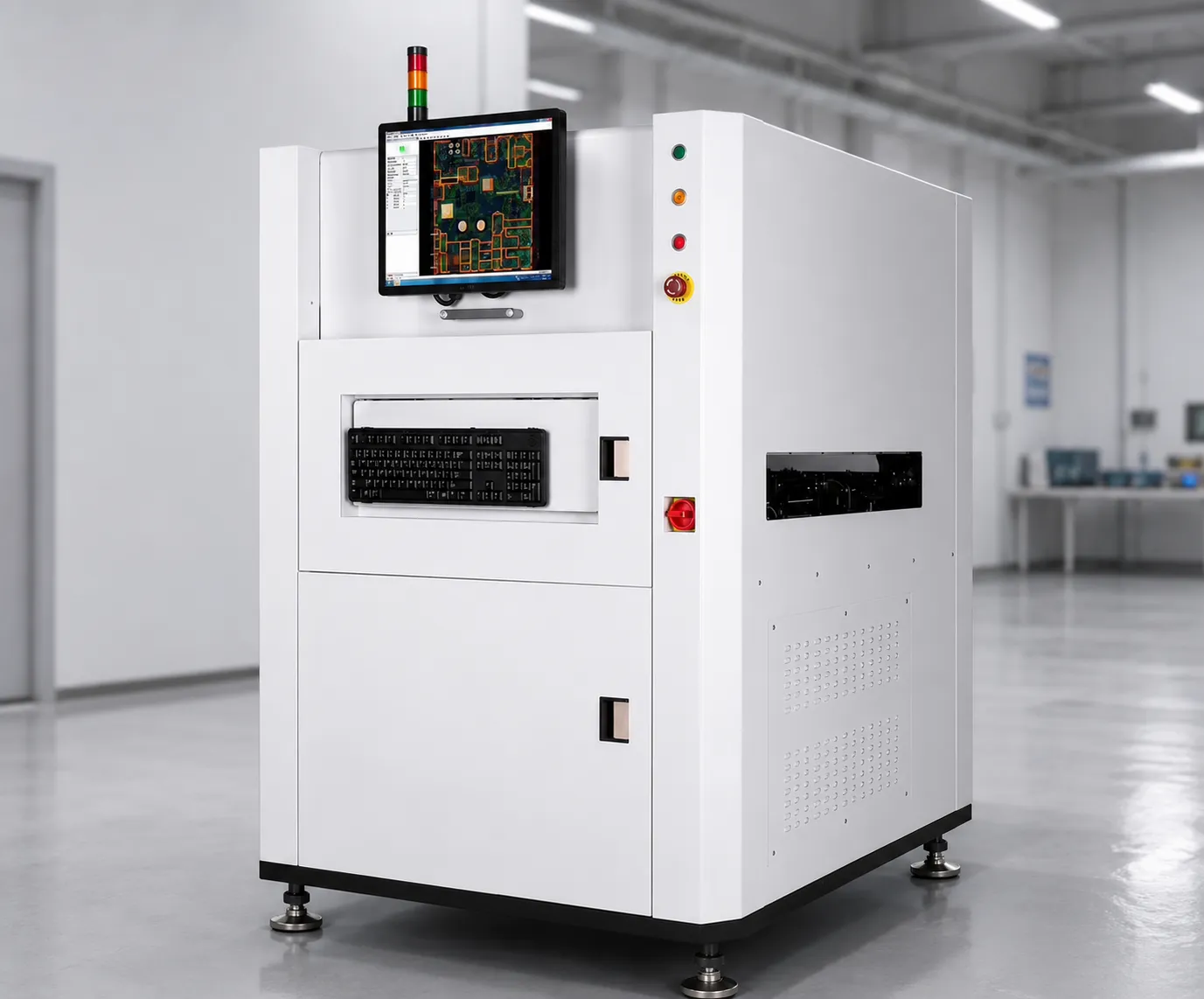
JHIMS XI-2000 AI-Powered SMT AOI Machine

Achieve 99.5% inspection accuracy with deep learning AI that reduces false positives by 95%. A 5MP industrial camera at 12µm resolution delivers 3-5 FOV/sec throughput, detecting 50+ defect types from 0201 chips to large BGAs — trusted by 2,456+ manufacturers in 30+ countries across automotive, consumer electronics and medical device industries.
🏅 ISO 9001 Certified
✅ CE Compliant
🌍 Serving 2,456+ Clients in 30+ Countries
🔧 36 R&D Engineers
📅 Est. 2012 — 14+ Years of Excellence


Explore JHIMS Solutions: Learn more about SMT assembly equipment and PCBA manufacturing solutions. Complete your quality gate with SPI inspection, AOI systems and X-ray inspection. Build the full line with solder paste printers, pick and place machines and reflow ovens. Support your line with feeders and feeder parts, SMT machine parts and sensors and industrial components. See how JHIMS supports why customers choose JHIMS, review our certificates and warranty policy, or explore buying guides, case studies and FAQ resources.

Pain Points & JHIMS Solutions

Common PCB Inspection Challenges

  • Manual visual inspection misses 5-15% of defects, especially on fine-pitch components (0201, 0.4mm BGA)
  • High false-positive rates (30-40%) with legacy 2D AOI systems cause unnecessary rework and line stoppages
  • Slow inspection cycles create bottlenecks — many systems only reach 1-2 FOV/sec on complex boards
  • Inability to detect 3D defects like insufficient solder volume, lifted leads and component warpage
  • No MES/ERP integration — quality data trapped in standalone machines with no traceability
  • Rigid programming requiring 4-8 hours of engineering time per new product introduction (NPI)

JHIMS XI-2000 Automation Solutions

  • 99.5% inspection accuracy with deep learning AI — catches the defects manual inspection misses
  • 95% fewer false positives — contextual AI distinguishes real defects from process variation
  • 3-5 FOV/sec throughput — never the bottleneck, up to 600 boards/hour
  • Optional 3D solder profiling detects insufficient solder, lifted leads and coplanarity issues
  • Standard MES/ERP integration via REST API and database connector for full traceability
  • AI-assisted NPI programming — new boards ready in under 30 minutes instead of 4-8 hours

Product Overview

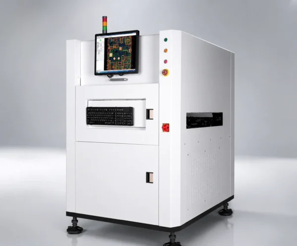
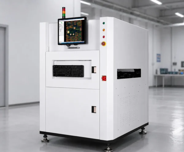
JHIMS XI-2000 automatic optical inspection machine

JHIMS XI-2000 AI-Powered SMT AOI Machine

The JHIMS XI-2000 is a next-generation inline SMT AOI machine that combines a 5MP industrial-grade Basler camera with deep learning AI to achieve 99.5% inspection accuracy. As an automatic optical inspection machine designed for high-mix, high-volume PCB assembly, the XI-2000 detects over 50 defect types across 0201 chips, fine-pitch BGAs, QFPs, connectors and through-hole components. At 3-5 FOV per second, this AOI inspection machine keeps high-volume SMT lines moving without sacrificing accuracy. Unlike conventional 2D AOI systems that rely on static rule-based algorithms, the XI-2000’s contextual AI engine learns from your production data to distinguish real defects from acceptable process variations. This reduces false positives by 95%, freeing engineers to focus on genuine process improvements.

Engineered with premium components from Basler (Germany), Panasonic/Mitsubishi (Japan), THK/HIWIN (Japan/Taiwan), and Keyence/Omron (Japan), the XI-2000 delivers industrial-grade reliability for 24/7 production environments.

Applications: Automatic optical inspection for automotive electronics, medical devices, consumer electronics, industrial automation, telecommunications, LED manufacturing, new energy/BMS, aerospace and defense, semiconductor packaging and home appliance PCB assembly.

📊 View Full Specifications

Key Features

🧠

Deep Learning AI Classification

Contextual AI engine trained on millions of PCB images reduces false positives by 95% compared to rule-based 2D AOI systems. It continuously learns from production data to adapt to process variation, board warpage and component tolerance changes without manual reprogramming.

📷

5MP High-Resolution Imaging at 12µm

Industrial-grade 5-megapixel Basler camera with telecentric optics delivers 12µm per pixel resolution across a 36.7×30.7mm field of view. Reliably inspects 0201 chip components, 0.3mm pitch BGAs and ultra-fine-pitch QFP leads that lower-resolution systems miss.

📐

Optional 3D Solder Profiling

Adds volumetric solder measurement for detecting insufficient solder, excess solder, lifted leads and component coplanarity issues — covering the 3D defects that pure 2D AOI systems cannot see.

💡

4-Channel High-Grayscale LED Lighting

Multi-angle illumination eliminates shadows on tall components and improves contrast for reflective leads, dark PCBs and low-profile parts. Each channel is software-tunable for per-board lighting recipes.

🔍

50+ Defect Types Detected

Detects missing parts, offset, polarity errors, bridges, insufficient solder, tombstones, lifted leads, foreign material, wrong components, solder balls, component cracks and PCB substrate defects — from 0201 chips to large BGAs.

🔗

MES/ERP Integration

Standard REST API and database connector push inspection data into MES/ERP for full traceability. Real-time SPC dashboards and defect pareto reports keep your quality team informed.

⚡

3-5 FOV/sec Inspection Speed

High-throughput inspection at 3-5 fields of view per second never bottlenecks your SMT line — up to 600 boards/hour depending on board complexity.

🛠️

Fast NPI Programming

AI-assisted programming with automatic component library matching cuts new product introduction from 4-8 hours to under 30 minutes for most boards.

Technical Specifications

Parameter Specification Parameter Specification
Model XI-2000 Online SMT AOI Maximum PCB Size 650 × 560 mm
Camera 5 MP Industrial Camera (Basler) Optical Resolution 12 µm
Field of View (FOV) 36.7 × 30.7 mm Inspection Speed 3-5 FOV/sec
Lighting System 4-Channel High-Grayscale LED PCB Thickness 0.6 – 6 mm
Top Clearance 45 mm Bottom Clearance 50 mm
Conveyor Height 900 ± 20 mm Conveyor Direction Left-to-Right (SMEMA standard)
Power Supply AC 220V, 50/60 Hz, 1.8 KVA Air Supply 5 bar (0.5 MPa)
Operating Temperature 5-40°C Operating Humidity 25-80% RH (non-condensing)
Machine Dimensions 1200 × 1200 × 1840 mm (L×W×H) Net Weight 900 kg
Communication Interface Standard SMEMA + RJ45 Ethernet MES/ERP Integration REST API, database connector
Defect Types Detected 50+ types (see detection section) Inspection Accuracy 99.5% (verified at 0201 capability)
False Positive Rate < 5% (with AI learning) MTBF 50,000 hours
3D Profiling (Optional) Solder height, coplanarity, warpage Certifications ISO 9001:2015, CE, RoHS

Machine Configuration — Premium Global Components

Every JHIMS XI-2000 is built with world-class components. We source only from industry-leading brands to ensure long-term reliability and precision.

Basler
🇩🇪 Germany
5MP Industrial Camera
Cognex
🇺🇸 USA
Vision Processor (Optional)
Panasonic
🇯🇵 Japan
Servo Motors & Drives
Mitsubishi Electric
🇯🇵 Japan
PLC Controllers & Automation
THK
🇯🇵 Japan
Linear Guides & Ball Screws
HIWIN
🇹🇼 Taiwan
Precision Linear Rails
SMC
🇯🇵 Japan
Pneumatic Components
Festo
🇩🇪 Germany
Pneumatic Cylinders & Valves
Keyence
🇯🇵 Japan
Fiber-Optic & Position Sensors
Omron
🇯🇵 Japan
Sensors & Detection

Applications & Industries

The JHIMS XI-2000 AI-Powered SMT AOI Machine is a versatile workhorse deployed across mission-critical electronics manufacturing sectors worldwide.

⚡
Automotive Electronics
🏥
Medical Devices
📱
Consumer Electronics
🏭
Industrial Automation
📡
Telecommunications
💡
LED Manufacturing
🔋
New Energy / BMS
✈️
Aerospace & Defense
💾
Semiconductor Packaging
🏠
Home Appliances

In-Depth Knowledge Hub


Industry-Specific AOI Solutions

Automotive Electronics (IATF 16949)

The XI-2000 meets rigorous automotive quality requirements with traceability to individual component level. It detects micro-cracks in MLCC capacitors, insufficient solder on high-current BMS traces and lifted leads on engine-control connectors. AI models are trained on automotive acceptance criteria including IPC-A-610 Class 3 and customer AQL limits.

Medical Devices (ISO 13485)

Medical electronics demand zero-defect manufacturing with complete traceability documentation. The XI-2000 records inspection images and results for every board, supporting FDA 21 CFR Part 11 electronic record compliance and full batch genealogy reporting.

Consumer Electronics

High-mix smartphone and wearable lines benefit from sub-30-minute NPI programming and 3-5 FOV/sec throughput. The AI engine distinguishes acceptable process variation from real defects on dense mainboards, cutting false calls that slow down operator verification.

5G Base Station & Telecom

Mission-critical telecom PCBs with large BGAs, high-pin-count connectors and mixed SMT/THT assembly demand zero-defect quality. The XI-2000 provides complete traceability at production volumes exceeding 50,000 boards monthly.

LED Manufacturing

LED driver boards and backlight strips benefit from 4-channel lighting recipes tuned for reflective aluminum substrates, eliminating false calls from conformal coating reflections.

New Energy / BMS

Battery management system PCBs require strict inspection of high-current traces and solder joints. The XI-2000 detects insufficient solder on thick copper traces and lifted leads on connectors with AI-verified confidence.

AOI Technology Guide

Understanding AOI inspection technology is essential for optimizing your SMT assembly process. Below is a comprehensive technical reference for engineers and process managers.

AI Classification vs Rule-Based 2D AOI

Rule-based systems flag anything outside static thresholds, causing 30-40% false positive rates. The XI-2000 contextual AI understands normal process variation — slightly darker solder joints, minor component color differences, normal placement tolerances — and reduces false positives by 95% while catching defects legacy systems miss.

Defect Detection Coverage

The XI-2000 detects 50+ defect types with AI-verified confidence: missing components down to 0201 size (99.8% confidence), component offset or misalignment from ±0.05mm (99.5%), polarity errors on 0201 markings (99.7%), solder bridges from 0.05mm width (99.3%), insufficient solder or dry joints (98.9%), tombstoning on 0201 parts (99.9%), bent or lifted pins on 0.3mm-pitch QFPs (99.2%), foreign material from 0.1mm particles (98.5%), wrong component values (99.0%), solder balls from 0.05mm (98.7%), component body damage from 0.1mm cracks (97.5%) and PCB substrate defects from 0.2mm scratches (97.0%).

4-Channel High-Grayscale Lighting

Four independently controlled LED channels at different azimuth angles eliminate shadows on tall components and maximize contrast for reflective leads, dark PCBs and low-profile parts. Lighting recipes are stored per board program and recalled automatically at changeover.

Optional 3D Solder Profiling

Adds true volumetric measurement of solder joints: insufficient solder, excess solder, lifted leads and component coplanarity. Combined with 2D inspection, the 3D channel detects defects that flat 2D imaging cannot resolve, such as gradated bridges and micro-cracks.

Manufacturing Best Practices Guide

Maximize your XI-2000 performance with these manufacturing operation and maintenance guidelines.

Fast NPI Programming

AI-assisted programming with automatic component library matching cuts new product introduction from 4-8 hours to under 30 minutes for most boards. The system generates inspection programs directly from CAD/Gerber data with minimal manual tuning.

MES/ERP Integration Setup

Standard REST API and database connector make integration straightforward. Inspection results, images and SPC data push into MES/ERP in real time, with support for forced-login operator tracking and full traceability reporting.

Calibration & Verification

Calibration targets ship with each machine for verifying optical resolution and lighting uniformity. Recommended verification: weekly resolution check, monthly full calibration with the NIST-traceable target, and quarterly Gage R&R study.

Production Workflow — XI-2000 in Your SMT Line

The XI-2000 is positioned post-reflow as the final quality gate before PCB unloading — catching all assembly defects before boards proceed to test, coating or box-build.

📦
PCB Loader
→
🎨
Printer
→
🔍
SPI
→
🤖
Pick & Place
→
🔥
Reflow
→
🔎
XI-2000 AOI
⭐ This Product
→
💻
ICT/FCT
→
🌿
Coating
→
📤
Unloader

The XI-2000 operates at 3-5 FOV/sec so it never becomes the bottleneck. Optional pre-reflow placement provides early defect detection, enabling rework before solder solidifies — valuable for high-value boards.

Manual Inspection vs. JHIMS XI-2000 — The Numbers Don’t Lie

Metric Manual Printing JHIMS XI-2000 Advantage
Inspection Accuracy 85-90% (fatigue-dependent) 99.5% 10-15% Higher
False Positive Rate 15-25% < 5% 80% Fewer False Calls
Inspection Speed (UPH) 60-120 boards/hour 300-600 boards/hour 5x Faster
Min Component Size 0201 (eyesight limit) 0201 (0.2×0.1mm) 4x Finer
3D Defect Detection Not possible visually Optional 3D profiling Infinite Advantage
Labor Cost/Month $2,100 (3 inspectors/shift) $0 — fully automated 100% Labor Saving
Traceability Manual paper records Full MES traceability Complete Digital Record
Shift Coverage Fatigue after 4-6 hours 24/7 continuous operation Non-Stop Operation
NPI Programming 1-2 days per product < 30 minutes 48x Faster

Based on typical industry benchmarks. Actual results may vary by application and operating conditions.

ROI Calculator — See Your Payback Period

Enter your current production parameters to calculate how quickly the JHIMS XI-2000 pays for itself.

Factory Tour — See JHIMS Manufacturing Excellence

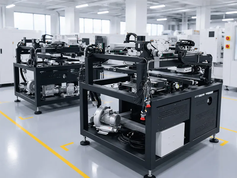
Every JHIMS machine is assembled, calibrated and burn-in tested in our Shenzhen facility, then carefully packed for international delivery.
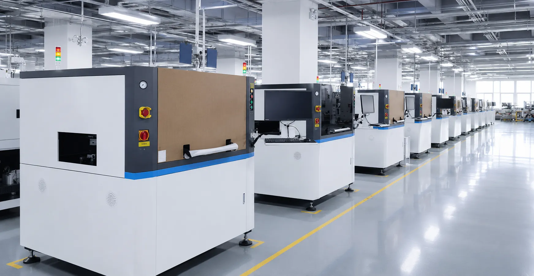
JHIMS manufacturing factory in Shenzhen

JHIMS Manufacturing Factory

JHIMS machine assembly workshop in Shenzhen factory

JHIMS Precision Assembly Workshop

JHIMS machine aging test workshop in Shenzhen factory

72-Hour Burn-In Validation

JHIMS machine demonstration workshop

Customer Demonstration & Application Lab

Product Videos — See the XI-2000 in Action

Watch the JHIMS XI-2000 performing real-world production tasks. All videos are hosted on YouTube for fast, reliable streaming worldwide.

AOI Machine for PCB Inspection: A Complete Guide
How Does an AOI Machine Detect Defects? — Tutorial
AOI PCB Inspection Machine Programming — Tutorial
AOI Automatic Optical Inspection Machine — Teaching

CUSTOMER SUCCESS STORIES

Trusted by SMT Factories Worldwide

Real-world results from SMT and PCB manufacturers who work with JHIMS — an ISO 9001 certified SMT equipment manufacturer — every case links to a verified JHIMS case study.
Frequently Asked Questions

🔧 Technical Questions

The XI-2000 reliably inspects 0201 chip components (0.2×0.1mm) at 12um resolution. It handles fine-pitch components down to 0.3mm pitch BGAs and 0.4mm pitch QFPs with full lead inspection capability. This is verified in 500+ global production deployments across automotive and consumer electronics manufacturing.

The contextual AI is trained on millions of PCB images and understands normal process variation. Unlike rule-based systems that flag anything outside static thresholds, the AI recognizes that slightly darker solder joints, minor component color variations, or normal placement tolerances are acceptable — not defects. This contextual understanding eliminates the vast majority of false calls that consume engineering time on traditional AOI systems.

The XI-2000 detects 50+ defect types including: missing components, component offset/misalignment, polarity errors, solder bridges/shorts, insufficient solder, tombstoning, pin/lead deformation, foreign material, wrong components, solder balls, component body damage, and PCB substrate defects. See our complete detection capabilities table in the specifications section for detection confidence levels for each defect type.

2D AOI uses top-down imaging to detect defects visible in a flat image — component presence, position, polarity, bridges, and visible solder quality. 3D AOI adds height measurement using structured light projection, enabling detection of insufficient solder volume, lifted leads, component coplanarity issues, and solder joint height variations. The XI-2000 offers 3D as an optional add-on module that can be field-upgraded without replacing the machine.

The XI-2000 operates at 3-5 FOV (Fields of View) per second. Each FOV covers 36.7×30.7mm. For a typical 200x150mm PCB, complete inspection takes approximately 15-25 seconds depending on component density and inspection settings. This speed keeps pace with SMT lines running at up to 5 meters per minute conveyor speed without becoming a bottleneck.

The XI-2000 supports PCB sizes from 50x50mm to 650x560mm with thickness from 0.6mm to 6mm. The large format capability makes it suitable for server motherboards, backplanes, and industrial control boards that exceed the capacity of smaller AOI systems (typically limited to 510x460mm). Top clearance is 45mm and bottom clearance is 50mm.

With the XI-2000’s AI-assisted auto-programming workflow, a complete inspection program for a typical 500-component board can be created in under 30 minutes. The process: import CAD data (2 min), load golden board image (5 min), AI auto-matches components to library (3 min), fine-tune critical components (10 min), validation on known-good boards (10 min). Compare to 4-8 hours on traditional AOI systems.

Yes. The XI-2000’s 45mm top clearance and 4-channel adaptive lighting enable inspection of through-hole components including connectors, electrolytic capacitors, transformers, and relays alongside SMT components. The system automatically adjusts lighting and inspection algorithms when transitioning between SMT and THT areas of the board.

The XI-2000 includes automatic warpage compensation that measures board flatness across multiple points and adjusts focus and inspection parameters accordingly. For flexible circuits and severely warped boards, the SMEMA-standard conveyor with adjustable support pins ensures flat presentation to the camera. Boards with warpage exceeding 1% of diagonal dimension may require fixture support.

Power: AC 220V, 50/60Hz, single phase, 1.8 KVA. Air supply: 5 bar (0.5 MPa) clean, dry compressed air. Operating environment: 5-40C ambient temperature, 25-80% relative humidity (non-condensing). The machine should be installed in a vibration-free location with adequate ventilation. A cleanroom environment of Class 100,000 (ISO 8) or better is recommended for optimal optical performance.

Pre-trained base models ship with the machine, covering common SMT component types and defect modes. During production, operator feedback (verify/override decisions) continuously refines the model for your specific boards. For unique components or customer-specific quality criteria, JHIMS application engineers can assist with custom model training using your golden board samples and defect examples. Models are managed through an intuitive interface requiring no machine learning expertise.

The 4-channel high-grayscale LED system captures images from multiple angles in rapid sequence, then computationally fuses them into a shadow-free composite. Each channel provides 256 grayscale levels (vs. 64 on budget systems). The adaptive lighting automatically sequences through different angles per component type, ensuring optimal contrast for each solder joint, component body, and PCB surface area — eliminating shadows that hide defects on tall components.

The XI-2000 provides a REST API and database connector for real-time integration with MES and ERP platforms. Inspection results, defect images, measurement data, and AI confidence scores are streamed to your MES with full traceability from component reel to finished board. The standard SMEMA interface handles physical conveyor integration, while the RJ45 Ethernet port handles data communication. Common MES platforms (Siemens, SAP, custom) are supported with configuration templates.

The XI-2000 is designed for post-reflow inspection as the primary quality gate, but can also be configured for pre-reflow inspection. Pre-reflow placement enables early detection of placement defects, allowing rework before solder solidification. Some customers deploy two units per line (pre and post reflow) for maximum process control. The auto-programming capability handles both pre and post-reflow inspection profiles seamlessly.
🛡️ Warranty & After-Sales

Standard warranty: 12 months covering manufacturing defects. Extended warranties of 24 or 36 months available. Support includes: remote diagnostics via secure VPN, cloud-based machine health monitoring, AI model updates, and access to JHIMS application engineering team. On-site service contracts available with guaranteed response times. All machines include 3 days of on-site installation and operator training. On-site service beyond the included days is available at a charge. Remote video training, documentation support and professional technical guidance are provided free of charge.

The JHIMS Cloud Platform provides real-time dashboards for yield monitoring, defect Pareto analysis, machine utilization tracking, and predictive maintenance alerts. Multi-factory views enable quality benchmarking across production sites. Data is transmitted securely via HTTPS with optional on-premise server deployment for customers with data sovereignty requirements. The cloud platform is included standard with every XI-2000 — no additional license fees.

The XI-2000 is manufactured under ISO 9001:2015 certified quality management. It carries CE marking (European Conformity) and RoHS compliance. The system can be validated to IPC-A-610 Class 2 and Class 3 acceptance criteria. For automotive customers, documentation packages support IATF 16949 compliance requirements. Complete certification documentation is provided with each machine shipment.

Yes. Standard deployment includes 3 days of on-site training: Day 1 covers operator-level operation including board loading, inspection start/stop, and defect review. Day 2 covers engineer-level programming including CAD import, AI model management, and inspection parameter optimization. Day 3 covers administrator functions including MES integration, user management, and maintenance procedures. Remote refresher training is available on demand.

With proper preventive maintenance and use of genuine JHIMS spare parts, the XI-2000 is designed for 8-10+ years of industrial service. The use of premium components (Basler cameras, THK guides, Panasonic servos, Mitsubishi PLCs) significantly extends operational life compared to budget alternatives. The 50,000-hour MTBF rating reflects real-world reliability across 500+ global deployments.

Yes. The XI-2000’s system supports remote desktop access for diagnostics and troubleshooting. With your permission, our engineers can connect remotely to diagnose issues, adjust parameters, update AI models, and install software updates — reducing downtime and eliminating travel costs. Remote support is available during Shenzhen business hours (UTC+8) with 24-hour emergency escalation for critical issues.

We recommend keeping: LED lighting modules (1 set), camera lens cleaning kit, air filters (set of 4), conveyor belts (2 pairs), calibration target, network cables, and a set of fuses. JHIMS offers a recommended spare parts kit at a discounted price with every machine purchase. Consumables like lens cleaning cloths and air filters should be replaced quarterly.

Yes, we offer annual preventive maintenance (PM) contracts that include quarterly remote health checks, annual on-site service by a JHIMS-certified engineer, calibration verification with NIST-traceable standards, software and AI model updates, and priority technical support with 4-hour response time. Contact our sales team for pricing in your region.
🚚 Shipping & Payment

Standard lead time is 6-8 weeks from order confirmation to shipment. This includes manufacturing, optical calibration, 72-hour burn-in testing, and final QC inspection. Rush orders may be accommodated for shorter lead times subject to production schedule availability. Contact our sales team for current delivery estimates based on your configuration requirements.

Standard payment: 70% T/T deposit with the order, 30% T/T before shipment. L/C at sight available for established customers. Shipping via sea freight (FCL/LCL) or air freight from Shenzhen. FOB, CIF, or DDP terms available. Complete export documentation provided including certificate of origin (Form E/F for tariff preferences), CE declaration, and ISO 9001 certificate.

Each XI-2000 is packed in a fumigated IPPC-compliant wooden crate with vacuum-sealed moisture barrier, shock indicators, and tilt indicators. The optical assembly is secured with custom-fitted foam supports and desiccant packs. Shipping crate dimensions are approximately 1500x1500x2100mm with a gross weight of approximately 1,100kg. Air-ride suspension trucks are recommended for ground transport to final destination.

JHIMS ships to over 30 countries worldwide including USA, Germany, India, Vietnam, Mexico, Brazil, Turkey, Thailand, Malaysia, and many more. Contact our sales team with your specific destination for shipping feasibility, transit time estimates, and any import/export restriction guidance. We have experience navigating customs requirements across all major electronics manufacturing regions.

Absolutely! We encourage factory visits to our Shenzhen facility. Tour our AOI manufacturing line, optical calibration cleanroom, and burn-in testing area. Bring your own PCB samples for a live demonstration on an XI-2000. Meet our engineering and applications team. Contact us to schedule a visit �� we provide airport pickup, hotel recommendations, and a complete factory tour experience.

The minimum order quantity is 1 unit. Volume discounts are available for orders of 3+ units. Multi-year framework agreements with scheduled deliveries can be arranged for large-scale deployments. Contact our sales team to discuss your specific requirements and volume pricing options.

Each shipment includes: commercial invoice, packing list, bill of lading/airway bill, certificate of origin (Form E/Form F where applicable), CE Declaration of Conformity, ISO 9001 certificate, user manual (English), installation guide, maintenance checklist, calibration certificates, and burn-in test validation report.

Import duties and taxes vary by country and are the responsibility of the buyer unless DDP terms are agreed. We can provide HS code classification (9031.49 for optical inspection equipment) and assist with customs documentation. For DDP shipments, we handle all import formalities and deliver to your facility with all duties and taxes paid. Contact us for a DDP quote to your specific destination.

Reference videos: watch the process on YouTube; watch the process on YouTube; watch the process on YouTube.

Weight 900 kg
Dimensions 1200 × 1200 × 1840 mm
Field of View (FOV)

36.7 × 30.7 mm

Maximum PCB Size

650 × 560 mm

Inspection Speed

3-5 FOV/sec

PCB Thickness

0.6 – 6 mm

Power Supply

AC 220V, 50/60 Hz, 1.8 KVA

Lighting System

4-Channel High-Grayscale LED