Address
Building A1, Runteng Industrial Park, No. 4 Xishan Road, Longteng Community, Shiyan Subdistrict, Bao'an District, Shenzhen 518000, China
Work Hours
Monday to Saturday: 09:00 – 23:00 (UTC+8)
Sunday: closed
Address
Building A1, Runteng Industrial Park, No. 4 Xishan Road, Longteng Community, Shiyan Subdistrict, Bao'an District, Shenzhen 518000, China
Work Hours
Monday to Saturday: 09:00 – 23:00 (UTC+8)
Sunday: closed

Request a quote
3D SOLDER PASTE INSPECTION
Eliminate 70% of SMT defects with true 3D solder paste inspection. The S630 combines industry-leading PSLM PMP projection technology with a 5-megapixel CCD, less than 5-minute Gerber programming, and a 10-year optical warranty — engineered for zero-defect SMT lines in automotive, medical, consumer electronics and LED manufacturing.
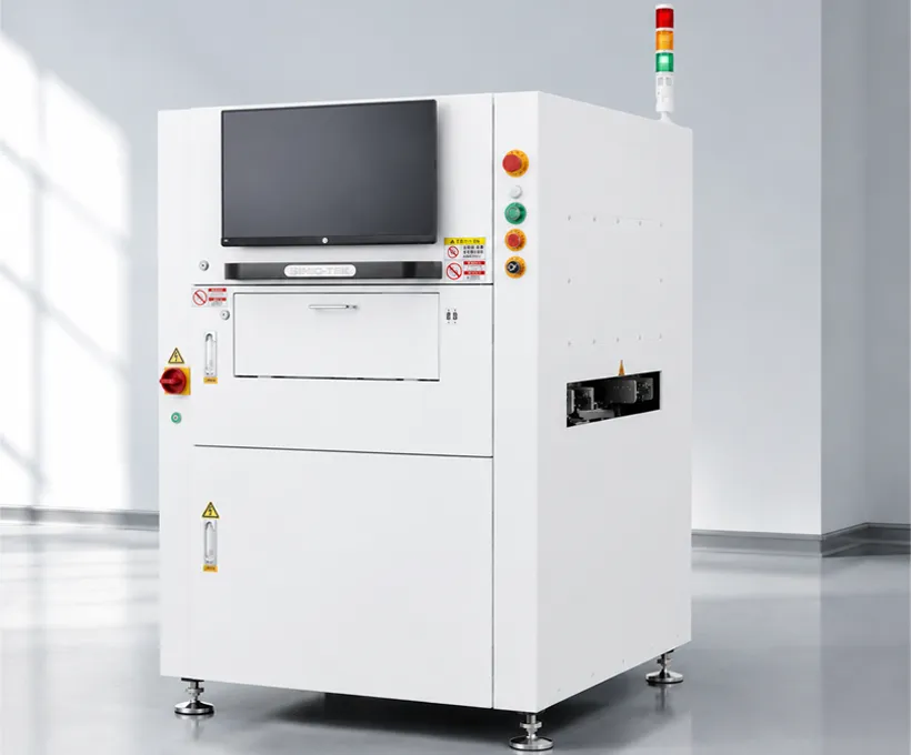
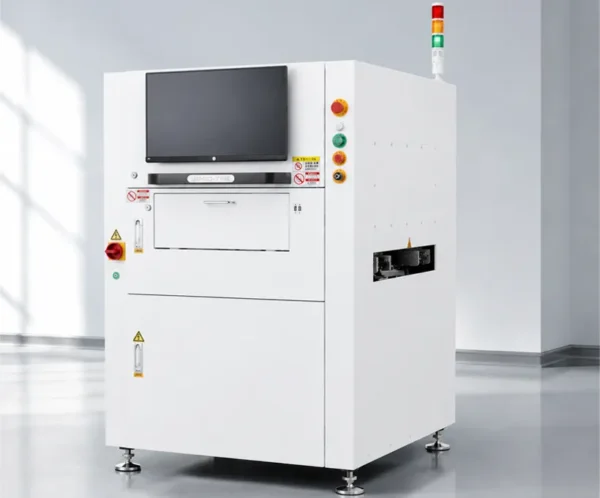
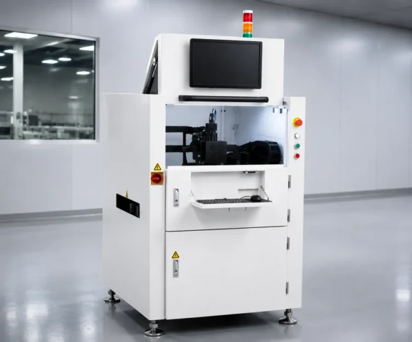
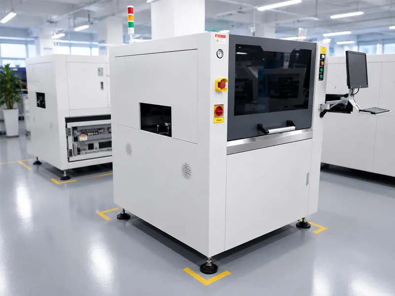
JHIMS S630 3D SPI Solder Paste Inspection Machine
The JHIMS S630 is a 3D SPI solder paste inspection machine engineered for high-volume SMT lines. As a 3D solder paste inspection system using PSLM PMP projection technology, the S630 delivers true 3D volumetric measurement of every solder paste deposit — volume, area, height, XY offset and shape — with sub-micron repeatability, catching defects before reflow to eliminate 70% of downstream soldering failures. The patented Synchronous Structured Light Technology resolves shadow effect interference, while dual RG (Red-Green) light sources handle high-contrast substrates including black PCBs and ceramic boards. A 5-megapixel industrial CCD camera supports fast, stable inspection down to 0201 components.
Engineered with premium components from Basler/Cognex (Germany/USA), Panasonic/Mitsubishi (Japan), THK/HIWIN (Japan/Taiwan), and Mitsubishi/Siemens (Japan/Germany), the S630 delivers industrial-grade reliability for 24/7 production environments.
Applications: 3D solder paste inspection for automotive electronics, consumer electronics, medical devices, LED manufacturing, new energy, industrial control, telecommunications and home appliance PCB assembly.
Software-defined grating with programmable phase shifts — zero mechanical wear, zero phase drift, and a 10-year free replacement warranty on the 3D projection head. Adjustable detection height from 550μm to 1200μm without hardware changes.
Industrial CCD camera paired with a premium telecentric lens. Supports 0201 component inspection at 13μm, 16μm, or 20μm resolution, with monochrome and color 2D imaging as standard.
100K-pad Gerber files converted in under 10 minutes. Direct dual-file merging without third-party tools, Manual Teach mode for non-Gerber boards, and mixed-side panel support.
Patented 8-frame acquisition (4 high + 4 low exposure) with selectable Black/Normal/Bright PCB modes. Perfectly handles ceramic substrates and dark PCBs that confuse conventional systems.
Color-filtered 2D imaging isolates solder paste from flux, white lines and debris, detecting bridges below 30μm that height-only algorithms miss. Color defect images make operator verification easy.
Patented 3-color structured light heads at 120-degree intervals capture multiple angles simultaneously, eliminating shadow artifacts on tall components. Configurable as single, dual, or triple head.
Real-time PCB warpage tracking with automatic servo feedback and a ±5mm dynamic compensation range. AI-enhanced warp prediction reduces false positives by 25% on flexible circuits.
Real-time SPC with X-bar, R-chart, Cp/Cpk analysis, multi-PCB view comparison, custom report formatting, histogram, normal distribution and trend analysis.
Auto-triggers stencil cleaning when missing prints are detected and transmits XY offset data to the printer for real-time correction. Proven integration with GKG and Desen printers.
Transmits defective board data to pick-and-place machines so they skip bad boards automatically — saving 30% mounting time on multi-panel PCBs. Camera-based barcode scanning included.
| Parameter | Specification | Parameter | Specification |
|---|---|---|---|
| Inspection Principle | Sinusoidal white-light projection PMP inspection | Industrial CCD Camera | 5 Megapixel |
| Resolution | 16 μm (13μm / 20μm optional) | 3D Projection Head | Projects periodic fringe patterns; true 3D imaging. 10-year free replacement warranty. |
| Monochrome 2D Image | Standard; facilitates operator defect confirmation | Color 2D Image | Standard; RGB synthesized color 2D images, more intuitive than monochrome |
| Z-Axis Real-Time Lifting | Standard; hardware compensation for board warpage during inspection | FOV Speed | 0.45s per field of view |
| Gage R&R | <10% | Conveyor Mode | Single lane (Dual lane available in D-series) |
| PCB Board Size (L × W) | 50 × 50 ~ 630 × 550 mm | PCB Thickness | 0.4 ~ 7 mm |
| X-Y Mechanism | Inspection head moves in X and Y axes; PCB remains stationary | Fixed Rail Side | Front rail fixed (Rear rail optional) |
| Rail Width Adjustment | Automatic and manual, two modes | PCB Positioning & Clamping | Edge positioning and clamping |
| Conveyor Height | 900 ± 40 mm | PCB Edge Clamping Width | 3 mm |
| Part Height Clearance | Top: 30mm / Bottom: 40mm | Minimum Pad Spacing | 150 μm |
| PCB Conveyance Direction | R→L or L→R; software one-key switching | Operating System | Windows 10 64-bit Enterprise Edition |
| Software Language | Chinese / English | Programming Software | Gerber (RS-274X, RS-274D), CAD |
| Programming Time | < 5 minutes | Program Fine-Tuning Time | < 5 minutes |
| Changeover Time | < 3 minutes | Panelized Program | Convenient panelized program creation (including mixed-side panels) |
| Data Input Types | Stencil file, Gerber (RS-274X, RS-274D); manual window addition supported | SPC Data Acquisition & Analysis | Production Trend, X-bar chart, R chart, Cp, Cpk. Records volume, area, height, offset per solder joint. Defect cause charts, full-board value images, normal distribution, individual component test data curves, real-time defect images. |
| Network Requirements | Supports TCP/IP protocol; real-time image transmission without affecting operation | CPU | Intel i7 |
| Memory | 24 GB (32 GB optional) | Hard Disk | 1 TB HDD / 1 TB SSD optional |
| Operating System | Windows 10 64-bit Enterprise Edition | Monitor | 24″ LCD Monitor |
| Input Devices | Mouse, Keyboard | Dimensions | W1180 × D1330 × H1530 mm |
| Air Supply Requirement | 4 ~ 6 Bar | Weight | 1,160 kg |
| Power Supply | 220 V, 10 A | Power Consumption (Startup / Normal) | Startup: 2.5 kW / Normal operation: 2 kW |
| Operating Air Consumption | 5 L/min | Floor Load Requirement | 450 kg/m² |
| Grounding Requirement | Ground wire required | SMEMA Interface | Equipped; provides good/bad board output signals |
| Safety Protection System | Comprehensive safety indication and interlock system | Barcode Scanning | Camera-based barcode |
| Auto/Manual Inspection | Both modes available | Technical Documentation | Complete technical, operational, and maintenance manuals (including electronic versions) and software installation media |
| Software Upgrade Service | Permanent, free software upgrade service provided | Standard MES System Integration | Standard MES system integration with Webservice API |
Every JHIMS S630 is built with world-class components. We source only from industry-leading brands to ensure long-term reliability and precision.
The JHIMS S630 3D SPI Solder Paste Inspection Machine is a versatile workhorse deployed across mission-critical electronics manufacturing sectors worldwide.
Full SPI-AOI closed-loop integration for engine control unit PCB assembly, with real-time SPC monitoring achieving CPK above 1.67 across 24/7 operation. IATF 16949-compliant traceability from solder paste print to final inspection keeps tier-1 automotive suppliers audit-ready.
High-precision 3D inspection for RF-sensitive boards with impedance-critical traces. PSLM technology handles large-format PCBs up to 630×550mm with consistent sub-micron repeatability across the entire board surface.
Under 3-minute changeover between product variants with PLC preset storage for up to 50 board types. Dynamic Mark Point recognition eliminates per-panel fiducial reading, saving 40% inspection cycle time on multi-panel arrays.
Cleanroom-compatible configuration with HEPA-filtered enclosure options, 100% traceability with barcode-to-SPC data linking, and validated inspection processes meeting FDA 21 CFR Part 11 electronic record requirements.
Dedicated L-series SPI for ultra-long LED strips up to 1.2 meters. D-Lighting technology handles reflective aluminum substrates, while RGB Tune filtering eliminates false bridges from conformal coating reflections.
Telecentric lens static compensation solves within-FOV warp variation, with dedicated FPC fixtures and vacuum clamping options. AI warp prediction reduces false positives by 25% versus standard Z-axis compensation alone.
Understanding 3D solder paste inspection technology is essential for optimizing your SMT assembly process. Below is a comprehensive technical reference for engineers and process managers.
Unlike traditional Moire systems that use physical glass gratings driven by piezoelectric actuators, JHIMS PSLM generates sinusoidal fringe patterns entirely through software. This eliminates 231 million mechanical drive cycles per year (calculated for 5K boards/day, 30 FOVs/board) — resulting in zero mechanical wear, zero phase drift, and a 10-year optical warranty.
The S630 captures 8 images per FOV — 4 with high exposure and 4 with low exposure. For black PCBs that absorb most projected light, the high-exposure group ensures sufficient signal; for reflective ceramic substrates, the low-exposure group prevents saturation. The algorithm intelligently fuses both groups into a single noise-free 3D reconstruction.
Conventional SPI systems detect bridging purely by height continuity between adjacent pads, which fails when flux residue or white silkscreen lines create height signals. JHIMS RGB Tune captures a color 2D image and filters by solder paste color (typically grey-metallic), ignoring non-solder height features — eliminating the number-one source of false bridge calls in production.
Three independently colored structured light projectors at 120-degree intervals illuminate the solder paste from different azimuth angles, creating three separate 3D reconstructions that are merged to eliminate shadow artifacts — particularly critical for tall components (up to 30mm top clearance) that cast shadows in single-projector systems.
Maximize your S630 performance with these manufacturing operation and maintenance guidelines.
Every S630 undergoes incoming QC (IQC), 5-axis CNC precision machining (±0.02mm), sub-assembly, final assembly with digital torque verification, 48-hour burn-in testing with 500-800 customer sample boards, 120-point final QC inspection, and vacuum-sealed export packaging with shock indicators.
Each machine runs continuously for 48 hours using customer-provided PCB samples (500-800 boards). Vibration stability, speed consistency, and false call rate are logged every 30 minutes. Only machines passing all 48 checkpoints receive a “Birth Certificate” shipped with the unit.
Daily: clean conveyor rails and verify SMEMA signals. Weekly: inspect and clean the 3D projection head lens with approved optical wipes. Monthly: verify calibration with a NIST-traceable standard board and run full Gage R&R. Quarterly: check pneumatic fittings, replace air filters, and verify grounding resistance.
JHIMS provides NIST-traceable calibration standards. The S630 achieves Gage R&R below 10%, height repeatability under 1μm (3σ), and volume/area repeatability under 1% (3σ). Annual recalibration service is available through our global service network or remote diagnostic tools.
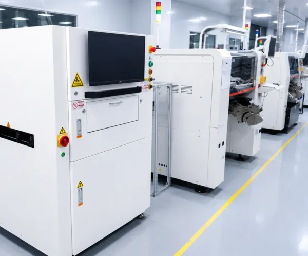
The S630 sits at the most critical quality gate in SMT assembly — immediately after solder paste printing. Catching defects here prevents 70% of downstream reflow failures.
The S630 closes the loop: it feeds XY offset data back to the printer for real-time correction and transmits Badmark information forward to the pick-and-place machine to skip defective boards — saving 30% mounting time on multi-panel runs.
| Metric | Manual Printing | JHIMS S630 | Advantage |
|---|---|---|---|
| Measurement Type | Subjective visual check / 2D area only | True 3D: Volume + Area + Height + XY Offset + Shape | S630 |
| Height Accuracy | Not measurable / Estimated from grayscale | <1μm repeatability (3σ) | True 3D |
| Volume Measurement | Impossible / Estimated (not true volume) | True volumetric measurement <1% repeatability | True 3D |
| Defect Detection Rate | 60-70% / 75-85% | >99% | True 3D |
| False Call Rate | N/A / 10-25% | <2% (with RGB Tune) | 5× Fewer Calls |
| Inspection Speed | ~2 min/board / ~30 sec/board | ~15 sec/board (630×550mm) | 5× Faster |
| Programming Time | N/A / 30-60 min | <5 min (Gerber import) | 5× Faster |
| Operators Required | 2-3 per line / 1 per 2 lines | 1 per 4+ lines | 4× Less Labor |
| SPC Data | None / Basic pass/fail | Full SPC: Cp/Cpk, X-bar, R, trend, histogram, defect pareto | S630 |
| Annual Mechanical Wear | N/A / Moderate | Zero (PSLM software-defined gratings) | S630 |
| Warranty | N/A / 12 months | 10-year optical + permanent free software upgrades | S630 |
Based on typical industry benchmarks. Actual results may vary by application and operating conditions.
Enter your current production parameters to calculate how quickly the JHIMS S630 pays for itself.
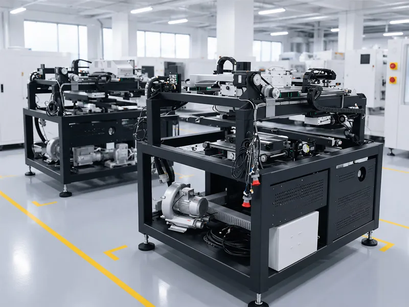
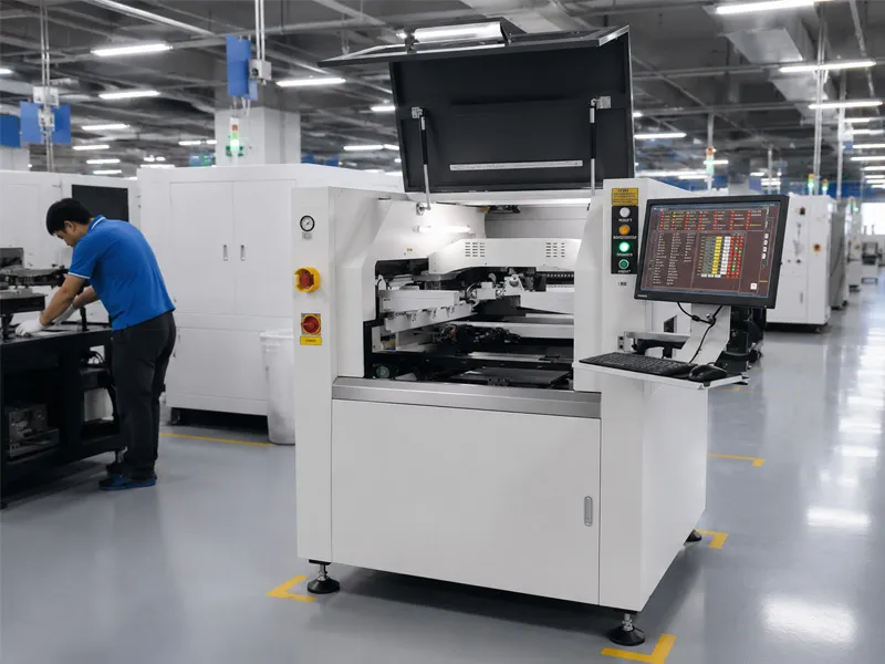
Every JHIMS machine is assembled, calibrated and burn-in tested in our Shenzhen facility, then carefully packed for international delivery.
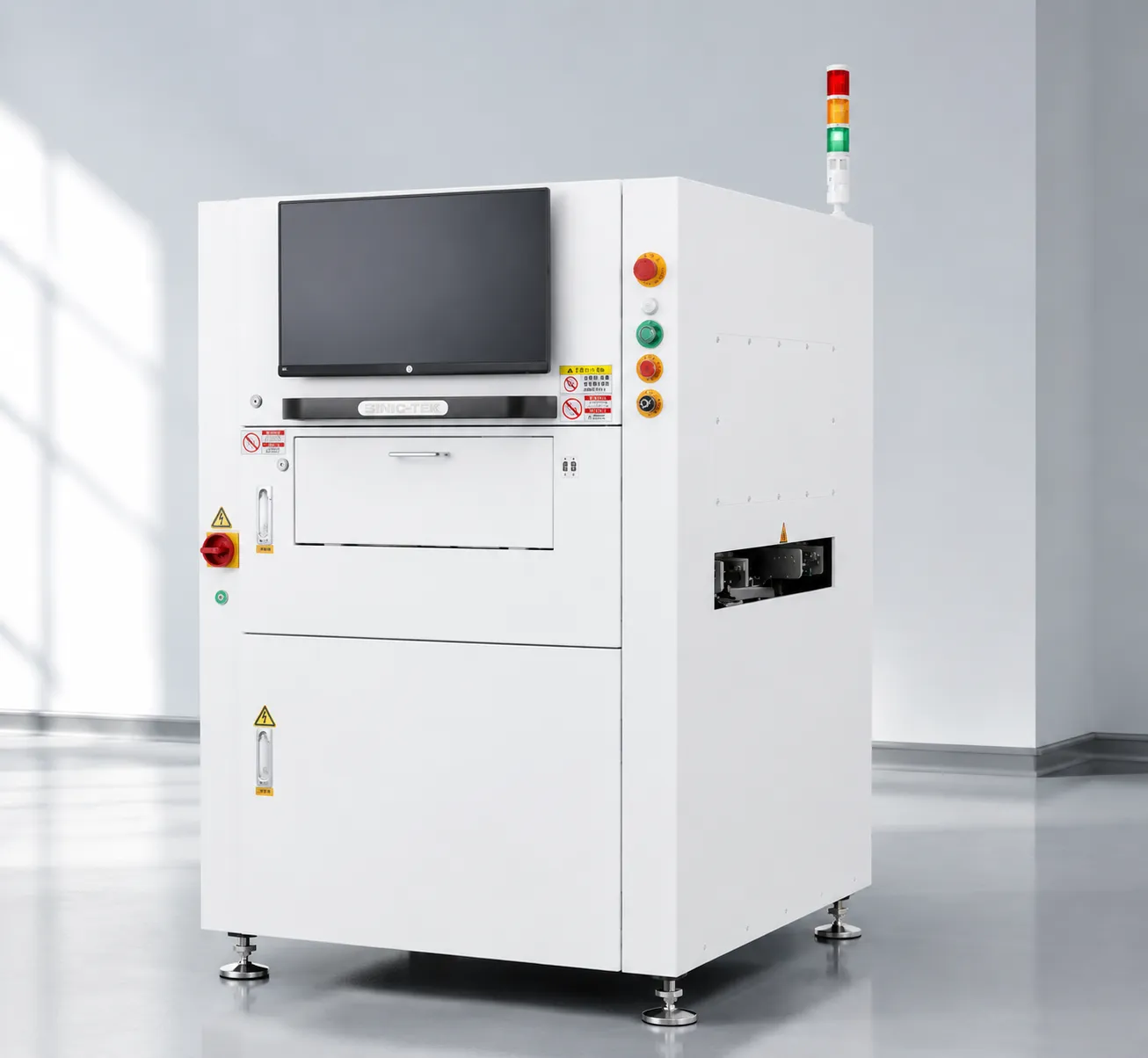
Watch the JHIMS S630 performing real-world production tasks. All videos are hosted on YouTube for fast, reliable streaming worldwide.
CUSTOMER SUCCESS STORIES
Real-world results from SMT and PCB manufacturers who work with JHIMS — an ISO 9001 certified SMT equipment manufacturer — every case links to a verified JHIMS case study.
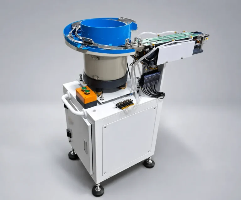 LINE AUTOMATION
How a TCL production line cut changeover time by 85% and lifted throughput by 30% with JHIMS automation.
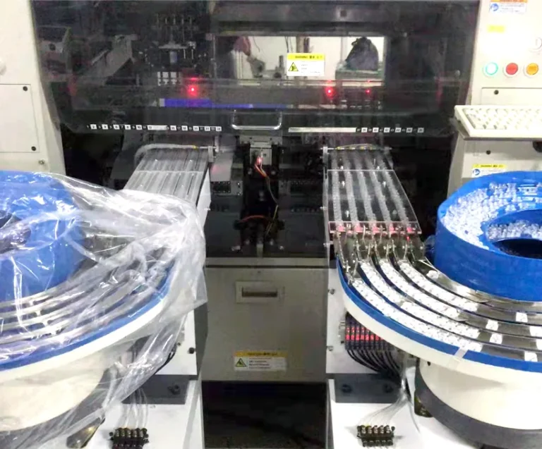 PCB ASSEMBLY
A Vietnamese EMS provider passed a Toyota supplier audit with zero scratch defects after reconfiguring their PCB line.
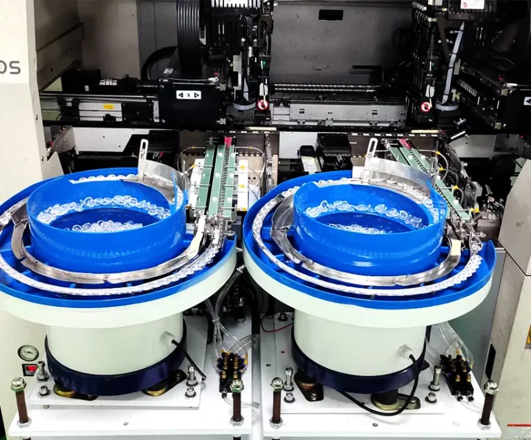 COST REDUCTION
How a Mexican PCB assembly operation reduced labor cost by 67% through SMT line automation.
LEARNING CENTER
Practical guides and real case studies about 3D SPI inspection and SMT quality control, written by JHIMS engineers — from procurement to line integration.
Reference videos: 3D Solder Paste Inspection (SPI): Ultimate Guide to High-Precision PCB Manufacturing; watch the process on YouTube; watch the process on YouTube.
| Weight | 1160 kg |
|---|---|
| Dimensions | 1180 × 1330 × 1530 mm |
| PCB Board Size (L × W) | 50 × 50 ~ 630 × 550 mm |
| PCB Thickness | 0.4 ~ 7 mm |
| Part Height Clearance | Top: 30mm / Bottom: 40mm |
| PCB Conveyance Direction | R→L or L→R; software one-key switching |
| Programming Time | < 5 minutes |
| Power Supply | 220 V, 10 A |
| Power Consumption (Startup / Normal) | Startup: 2.5 kW / Normal operation: 2 kW |